There are a number of terms that you will likely come across when you dive further into the world of electrical design, and one of the most prevalent will be a PCB. These are a fundamental part of the majority of electrical items that we use in our everyday life, such as laptops, phones, and computers. As such, if you want to work more in electronic design, then you should be sure to consider the below article, as this will discuss what a PCB is in more detail.

What Is It?
PCB stands for printed circuit board, and this is an electronic assembly that uses copper conductors in it in order to establish an electrical connection between various components. These boards are able to provide mechanical support between various electrical components so that it is possible for a device to be mounted within an enclosure. A specific number of steps need to be included within the design of a circuit board which will align with its manufacturing process and structure of the integrated circuit packaging.
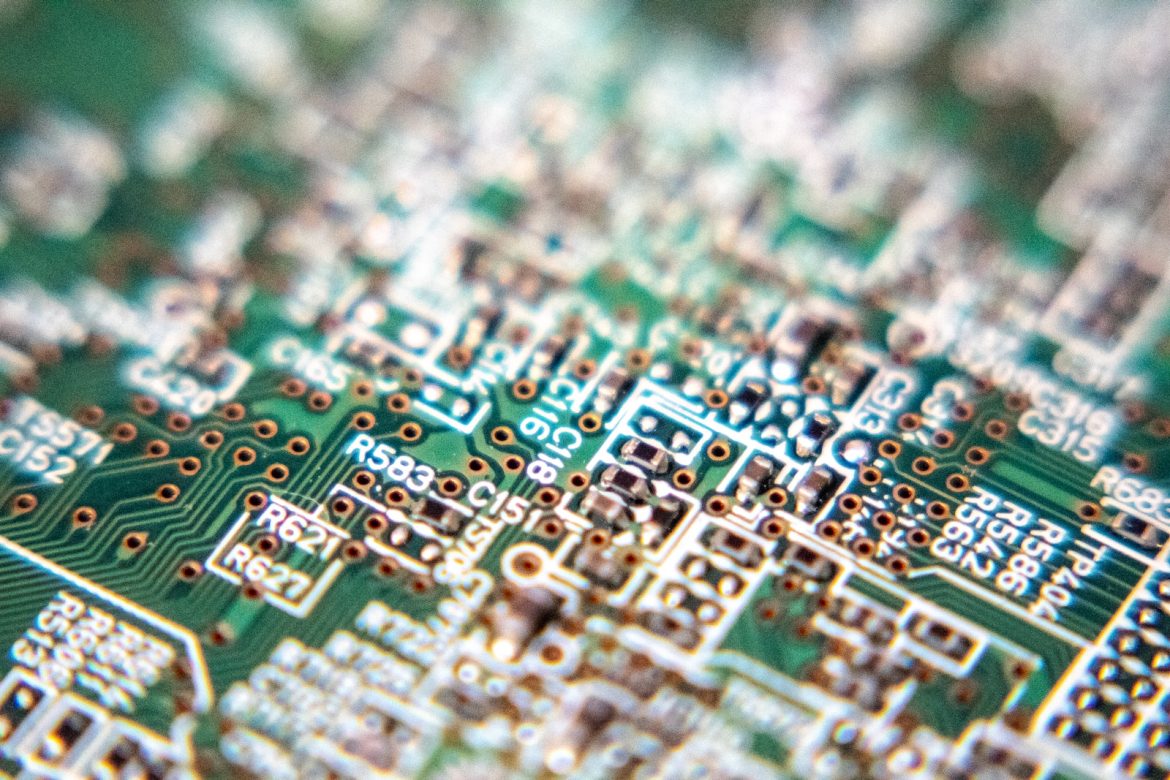
There are a number of conductive features which can be found on a PCB, and these include copper traces, conductive planes, and pads. In terms of the actual mechanical structure of a PCB, this is made up of an insulating material that is laminated between different layers of conductors. Overall, the structure is plated and then covered with a non-conductive solder mask, as well as a silkscreen material which is printed on the top in order to give a legend for some of the electronic components within the PCB.
The PCB design has developed within the electronics industry with changes in software and other technologies driving progress. The development is needed due to the massive part that they play in electrical interconnections that happen between components. Even PCB’s which are quite basic, need to be designed very carefully so that they will fulfill their function and be encased in the right way; if not, then they are not going to operate well.
Different Types of PCB
There are a few different types of PCB that get constructed on a daily basis. These are made out of a range of possible materials and are used for a variety of reasons. They include but are not limited to:
- Single-Sided PCB: When a PCB is single-sided, it means that it only has components which are mounted on one surface. The back surface tends to be fully copper and is also coated with a solder mask.
- Double-Sided PCB: When it’s double-sided, there are components mounted on both surfaces. Each one is defined as a single layer in the PCB stack-up, and as such, the surfaces tend to contain traces that will carry signals between various components.
- Multi-Layer PCBs: A multi-layered PCB will have a conductor on internal layers that are responsible for carrying electronic signals between the different components which are on there. Alternatively, the internal layers could also be conductive plane layers too. Each layer can be either single or double-sided.
- Rigid PCBs: These boards are unique as they are not only fabricated but also assembled on a rigid laminate material. There are a number of different types of rigid laminate material, but one of the most popular is FR4-grade epoxy resin-impregnated fiberglass.
- Rigid-Flex PCBs: These PCBs differ as they use a flexible polyimide ribbon that connects multiple rigid sections within a printed circuit board assembly. These are used for a number of different reasons, but one of the most common is when they have been placed on a moveable element like on a bending or folding enclosure.
- Flex PCBs: When a PCB is fully flexible, it means that there are no rigid materials in place and they are designed and manufactured purely on a flexible ribbon. They can have components mounted and soldered on them in the same way that a rigid board does, just without the actual rigid elements.
The Definition of a PCB Layout
It’s important to understand what the definition of a PCB layout is, especially if you intend to begin to design them and share those designs. A PCB layout is a CAD drawing that shows the location of all of the different elements that are going to appear when properly assembled on the printed circuit boards. All components are included on this, which includes the copper which is going to appear on both sides of the PCB.
